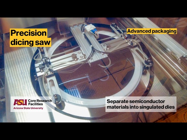
ASU Core Facilities Equipment Showcase: Precision dicing saw
Watch on YouTubeVideo summary
Advanced packaging relies fundamentally on precision, a requirement that becomes critical when wafers and semiconductor materials must be separated into individual dies. Even minor variations in the cutting process can negatively impact subsequent steps, making accuracy essential for maintaining high-quality standards throughout production. The featured dicing saw addresses these challenges by delivering precise and repeatable singulation capabilities across a wide range of materials, including silicon, molded cores, and other semiconductor substrates.
A key advantage of this equipment lies in its ability to ensure precision alignment, which guarantees accurate blade placement even on patterned wafers where intricate designs are present. Furthermore, the machine's dual blade configuration supports multiple dicing techniques, offering researchers significantly greater flexibility in their experimental workflows. This versatility allows users to adapt the tool for various specific needs without compromising on the high level of detail required for modern semiconductor applications.
The capabilities of this system extend from handling native 300 mm silicon wafers used in fan-out wafer-level packaging to producing extremely small individual samples measuring less than 1 mm by 1 mm. Such a broad range demonstrates the tool's adaptability for both large-scale industrial processes and delicate research tasks involving micro-scale components. By accommodating such diverse scales and material types, the dicing saw serves as a versatile asset that bridges the gap between high-volume manufacturing and specialized scientific inquiry.
Ultimately, this equipment represents a significant advancement for facilities requiring reliable and accurate separation of semiconductor materials. Its design ensures that every cut meets strict precision standards, thereby minimizing errors and enhancing overall process efficiency. Researchers and engineers can leverage these features to explore new packaging technologies with confidence, knowing that the underlying dicing process will support their most demanding projects. For those interested in learning more about how this technology supports advanced research initiatives, additional information is available through the provided institutional resources.
Read the full video transcript
Advanced packaging [music] depends on
one thing above all, precision. When
wafers [music] and semiconductor
materials need to be separated into
individual dies,
>> [music]
>> even a small variation in the cut can
affect the next step in the process.
This dicing saw provides [music]
precise, repeatable singulation across
silicon, molded core, and other [music]
semiconductor materials.
Precision alignment ensures accurate
blade placement across [music] patterned
wafers, while a dual blade configuration
supports multiple dicing techniques.
For researchers, that means greater
[music] flexibility.
From dicing native 300 mm silicon wafers
[music] for fan-out wafer level
packaging to producing individual
samples smaller than 1 mm by 1 mm.
Discover more at cores.research.asu.edu.
[music]